PS3 Architercture - An Overview
PS3 Architecture : An overview
I’m back with some interesting story about the cell processor.
The Cell Broadband Engine is a first of it’s kind SOC. It has multiple processing units like an embedded DSP like processor system - Processor for high performance pipeline configuration and high speed shared memory system with independent cache systems. This is Processor is regarded powerful than the intel i-9900k by some of the developers at Killzone.
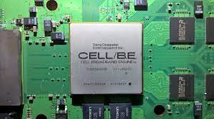
Let’s take a look at the processor first :
Let’s zoom in a bit shall we?
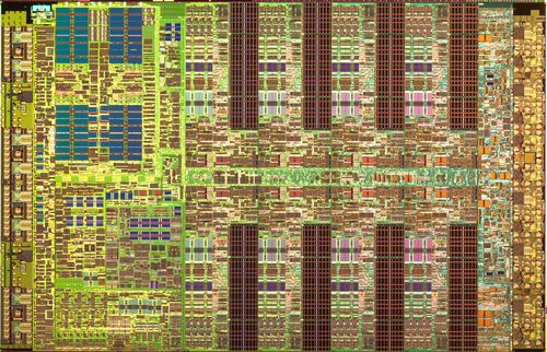
Whoahhhhh!!! that’s a lot of stuff isn’t it?. Don’t worry, I got you covered. Here is the simplified architecture diagram of the CBE - cell broadband engine. I tried to simplify it as much as possible to make the first encounter with this beautiful machine as pleasant as possible and still get a good understanding of the CBE and what make it that powerful.
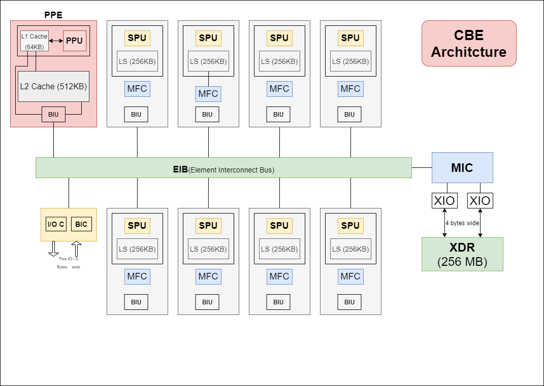
Note:- From now in the rest of the article I will be addressing the Cell Boroadband Engine as CBE.
The main parts of the CBE are :
- PPE - Power PC processing Element
- Eight SPEs - Synergistic processing Element (2 Are reserved for the OS operation in the PS3 and 6 are available for the applications)
- IOC + BIC (Dedicated high speed I/O controller and Bus interface controller for external devices and memory)
- MIC - High speed shared and coherent Memory Interface Controller
- EIB - Proprietary shared bus for connecting all elements together
Understanding the PPE - Power PC Processing Element
At its heart is the Power Processing Element, or PPE, featuring a 3.2GHz, 64-bit dual-core CPU based on IBM’s PowerPC 2.02 ISA (Instruction Set Architecture). It also supports SIMD extension and VMX upto SSE4.The PPE has a 32KB 2-way set associative L1 instruction cache, a 32KB 4-way set associative L1 data cache, and a 512KB 8-way set associative L2 instruction-and-data cache. The L1 data cache is controlled according to the write-through policy, and the L2 cache according to the write-back policy.
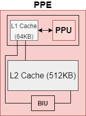
The PPE supports logical partitions (LPARs). An LPAR runs multiple independent operating systems simultaneously on a single CBE chip by supporting the Hypervisor, which has higher execution rights than normal operating systems. Hence the supervision mode and Hypervision mode of the CellOS.
The PPE supports multithreading. The main pipelines are single-threaded but have two threads’ worth of register files and other resources so that two threads can be executed simultaneously without overhead for context switching.
Understanding the SPE - Synergetic Processing Element
Each SPE is composed of an SPU and an MFC. The SPU is a processor core with a SIMD instruction set that handles 128-bit data. The SPU also has a 256KB local memory (local storage: LS) instead of a cache hierarchy. Programs executed by an SPE and all data accessed by load/store instructions are placed in LS. Data transfers between LS and external memory are conducted by MFC, a unit separate from the SPU.

The overall characteristics of SPU operation pipelines are as follows:
- 2 instructions issued per cycle
- 128-bit data bus
- 1 128-bit logical operation per cycle
- 4 parallel single-precision floating-point multiply-add operations per cycle
- 4 parallel 32-bit ALU operations per cycle
- 4 parallel 16-bit integer multiply-add operations (32-bit output) per cycle
- 8 parallel 16-bit ALU operations per cycle
- 16 parallel application-specific 8-bit integer operations per cycle
- 2 parallel 64-bit double-precision floating-point multiply-add operations per 7 cycles
- Latency
- 6 cycles for loads
- 3 cycles for integer operations
- 7 cycles for single-precision floating-point multiply-add operations
- 13 cycles for double-precision floating-point multiply-add operations
IOC + BIU
(BIF) or an I/O bus (IOIF) depending on the mode switch. The bus width can be adjusted in byte units. BIC is the running controller when Flex I/O is in BIF mode; IOC is the controller in IOIF mode. In this document, only IOIF will be discussed. I/O devices such as the network adaptor, graphics controller, and HDD controller, are connected to the CBE via IOIF. When thus connected, I/O devices with bus master functionality can access memory spaces inside the CBE directly, and internal CBE masters (PPE and SPE) can directly access the I/O devices connected to the IOC.
MIC - Memory Interface Controller
The main memory of CBE is XDR DRAM, which is directly attached to the CBE on an 8-byte wide XDR DRAM interface (two 4-byte wide ports). Though the specifications of the XDR DRAM interface allow up to 24 memory devices to be connected, configurations that are actually usable will depend on the specifications of the usable XDR DRAM memory devices. MIC is a memory interface unit including the XDR DRAM memory controller. It receives memory access requests from EIB and carries out buffering, scheduling, and data transfers.
EIB - Element Interconnected Bus
The internal modules of CBE — PPE, SPE, and others — are connected via EIB. EIB comprises a tree-structure command bus and a fourfold-ring-structure data bus. When access requests generated per master device reach the root of the tree-structure bus.
Closing notes
Well that’s it for now, I hope you understood the building blocks of the PS3 processor that led to all the magic. In the coming articles we’ll delve deeper deeper into the each component and explore their hardware pipeline and their Instruction Sets. Getting a strong understanding of the hardware is a crucial step to get the full power out of this Processor. Goodbye until next time!